The World of MEMS
The Enchippening of the Analog
What is MEMS?
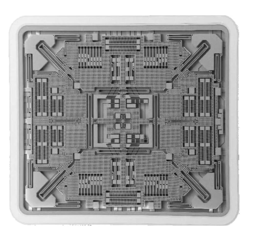
MEMS stands for “microelectromechanical systems”, which is a bit of a mouthful, but it means just what it sounds like. Microscopic devices, which contain both electrical and mechanical components.
Electrical components are like wires, resistors, transistors, capacitors, and so on. Mostly they can be made of flat layers of conducting, semiconducting, and/or insulating material, and thus can be straightforwardly manufactured on chips at scale using the fabrication technology of the semiconductor industry.
Mechanical components are tiny machines. Cantilevers. Vibrating diaphragms. Springs. Gears.
What can you use these for?
A miniature cantilever can be used in:
accelerometers and pressure sensors
force on the cantilever is converted to electric current using the piezoelectric effect
electrostatic actuators
the cantilevered electrode bends towards the fixed electrode in the presence of a voltage
this is used to tilt micromirrors in arrays
used in optical switching for fiber optic networks
and potentially LIDAR
and spectroscopy
Piezoelectric devices can also be used in
microphones and amplifiers
pressure from sound waves is converted into electric current
ultrasound transducers (for sensing and emitting ultrasound waves)
oscillators (for clocks)
Combining cantilevers and piezoelectric components can produce magnetic field sensors.
A microbolometer, a microscopic heat sensor, involves a temperature-sensitive material suspended over a reflector
So, basically, MEMS allows devices to sense and respond to mechanical signals (pressure, acceleration, vibration, sound and ultrasound), as well as make other measurements (magnetism, temperature, chemical composition, optical imaging, and time).
How Are MEMS Devices Made?
The basic fabrication technologies for MEMS are the same ones used for semiconductor devices.
MEMS components aren’t quite made of flat rectangles layered on top of each other, but they’re close.
A cantilever can be made by depositing a layer of “sacrificial” material, then a structural layer for the “arm”, and then dissolving away the sacrificial material with a strong etchant (like hydrofluoric acid), leaving the arm to balance over the substrate with a gap between.
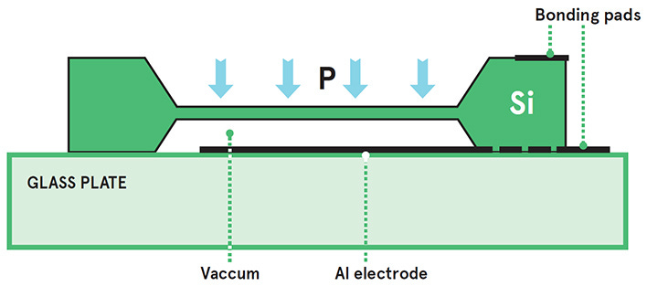
Likewise, a capacitor, which involves two layers separated by a vacuum, can be produced by depositing and patterning the electrodes and a sacrificial layer between them, and then etching away the sacrificial layer, leaving two capacitor plates separated by vacuum.
There are some more exotic methods used for high aspect ratio features, but basically you make MEMS chips using the same techniques you use for other kinds of semiconductor chips.
What’s New in MEMS?
MEMS devices are old; the first one was developed in 1968 by Harvey C. Nathanson at Westinghouse, as a cantilever-based tuner for radios.
MEMS components were behind the inkjet printers of the 1980’s and the automotive inertial sensors of the 1990s.
So what’s the new part? Here are a few (of many) things that have improved in MEMS in recent years.
Foundries
A “foundry” is the semiconductor industry’s term for a manufacturing service. A foundry manufactures chips that other companies design.
Foundries make it much easier to start a new chip company — all you need is a new design, not the capital expense and manufacturing know-how needed to build and operate your own fab. For specialty applications, such as biomedical sensors, decoupling application expertise from manufacturing expertise seems especially important.
The first MEMS foundry was offered by Olympus, the Japanese camera and optics company, back in 2002.
Piezoelectric MEMS foundries are even newer; the first was Rohm, another Japanese manufacturer, which opened up its production lines to customers in 2014.
As late as 2014, only 20% of MEMS production was outsourced to foundries.
PMUTs and CMUTs: Ultrasound on a Chip
PMUTs (piezoelectric micromachined ultrasound transducers) and CMUTs (capacitative micromachined ultrasound transducers) are microarrays of tiny MEMS ultrasound sensors and transmitters. Each is made of a flexible membrane over a substrate, that generates a change in current when it is exposed to ultrasonic waves.
While the first commercial CMUT device dates back to Hitachi’s 2009 “Mappie” probe, the performance of these devices spiked in the late 2010’s due to innovation in materials and deposition techniques.
MEMS on-chip ultrasound allows miniaturizable, portable or even wearable medical ultrasound devices, as we’ll see in a later post.
Speakers and Microphones
The first monolithic (all-silicon) MEMS speaker was only launched in 2020. MEMS speakers can be smaller and more durable, allowing them to be used in hearing aids.
New piezoelectric materials for MEMS-based speakers and microphones have come out in the past few years, reducing size and cost.
RF Switches
Radiofrequency switches made from MEMS electrostatic actuators are just beginning to hit the smartphone market this decade after many years of development.
Compared to semiconductor switches, MEMS switches have lower power consumption and less signal leakage — which means fewer dropped calls and longer battery life.
Why do We Care?
Anything that can be manufactured on a chip can be miniaturized, integrated with electronics, and made cheaper and more abundant year after year.
MEMS technologies expand the range of “what can we do on a chip” beyond the straightforwardly electronic to the world of other physical forces — mechanical pressure, sound, temperature, even chemical composition.
A world where we can sense more is a world with better health (through noninvasive diagnostics) and more efficient industry (through tracking more measurements and adjusting processes accordingly, and through greater automation.) MEMS makes the analog world, not just the digital one, accessible to massive scaling effects.


You mentioned gears in MEMS, do any MEMS applications actually use gears? I’ve only heard of beams and membranes, basically just vibrating elements.