What’s Up With Exponential Tech Improvement?
If there’s one thing that keeps getting better, it’s computer chips, right?
Transistors keep getting smaller, so each chip has more transistors. A chip with more transistors can do more computation in a given time. (I wrote an article in Asterisk Magazine earlier this year about what Moore’s Law means for predicting progress in AI.)
But where does Moore’s Law come from, anyway? Why is our technology industry so good at making smaller and smaller chips over time?
And, in general, why do some technological industries advance at a breakneck pace while others stagnate?
The cost of sequencing a human genome, for instance, has also been falling exponentially over time.
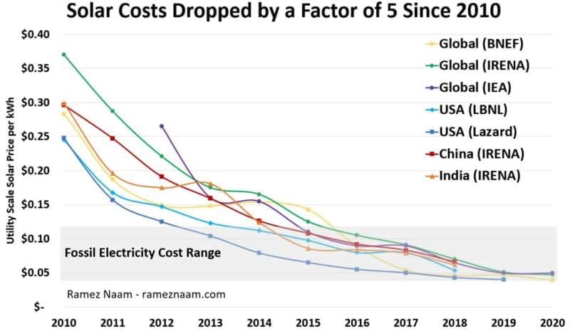
And so has the cost of energy from solar panels:
Is this some kind of universal “law” of technology development? Is “exponential” improvement just how technology evolves generally, in some Kurzweilian sense?
Or are these just three unrelated, hand-picked examples, which likely have different explanations?
An alternative (oversimplified, but I think directionally correct) narrative is much simpler:
Every tech that is improving exponentially in the 21st century is explained by improvements in semiconductor fabrication.
Solar panels and genomic sequencing devices are made using very similar equipment and processes as those used to make computer chips. When semiconductor manufacturing advances, so does the manufacturing of everything you can put on a chip.
And, of course, any technology that is downstream of such manufacturing will improve as a consequence. mRNA vaccines, for instance, are only possible because of ubiquitous genetic sequencing.
A Very Basic Introduction to Semiconductor Fabrication
If you look up introductory materials on “how computers are made”, you’ll typically get an introduction to the physics of semiconductors, and maybe a graphic with some electrons moving around. Or maybe you’ll get an introduction to logic gates and how you can represent any computation with circuits built of “AND”, “OR”, and “NOT” operations.
But that only tells you the principles of how a computer works. It doesn’t tell you how a computer is made.
Fundamentally, computer chips are made by putting flat layers of stuff on top of other flat layers of stuff.
This is a cross-section of a MOSFET, the most common type of transistor used in computers today.
A transistor is essentially a switch without moving parts.
Current can flow from the source to the drain, or not; it depends on whether the gate is “open.” And the gate is “open” or not depending on the voltage applied between the source and the gate.
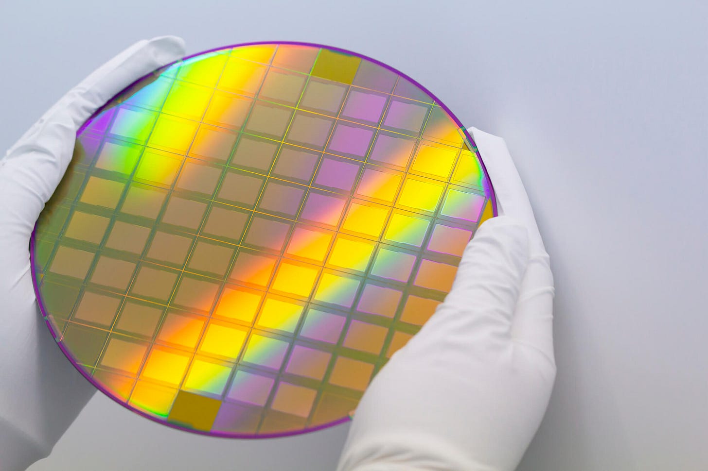
But never mind how it works, for now. We care about how it’s made. And it’s made of microscopically thin, flat layers of semiconductors, insulators, and metals, deposited or grown in a pattern on a flat wafer.
Putting transistors together into circuits is just more of the same thing: you’re laying flat rectangles of stuff on top of other flat rectangles of stuff.

All of those layers are produced by basically two mechanisms: deposition and etching.
Depositing a thin, perfectly even, uncontaminated, often crystalline layer of stuff on a wafer requires extreme precision. Typically you have to vaporize the stuff and either let it physically condense onto the surface or chemically bond to the surface.
If you want it to have a crystalline structure (and you do, for many of these materials), you need a perfect molecular lattice grown layer by layer without irregularities, which is known as epitaxy.
There’s a whole zoo of different methods of epitaxy and thin film deposition used for different materials, and these methods are not at all confined to semiconductors — they’re used for all kinds of thin precise coatings.
To make a pattern, the layer then has to be etched away everywhere except the intended rectangles.
This is where photolithography comes in. A light-sensitive material (photoresist) is applied to the wafer, and UV light is projected in precise patterns, so that the photoresist hardens where it’s exposed to light and can be removed elsewhere. Once you have the pattern physically layered onto the wafer, you can etch the exposed areas away, with corrosive chemicals or (more commonly today) with plasma ions.
The details are complex, but the fundamental techniques are always:
lay down a perfectly flat, pure layer of stuff;
etch it away where you don’t want it.
And, fundamentally, Moore’s Law is about semiconductor manufacturers getting better at making smaller rectangles of flat stuff.
Of course, how to do this is almost impossibly complex, and involves many independent innovations in many fields.1
But at a high level, that’s what semiconductor fabrication is: endless intricate variations of spraying vapor or plasma on stuff, letting it cool, and doing it all over again.
Beyond Computers: Other Semiconductor Devices
What else is made with these techniques?
For one thing, lots of devices besides computer chips are semiconductor devices.
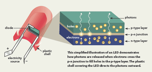
An LED, for instance, is an extremely simple semiconductor device: just one layer of p-type and one layer of n-type semiconductor.
When electrons flow from the electron-rich n-type layer to the electron-poor p-type layer, light is emitted.
The materials for LEDs such as those used in TV, computer monitor, and cell phone screens are somewhat different from those used in microprocessors, but they are still laid down using vapor deposition techniques.
Likewise, a laser diode is a semiconductor device made of a single p-n junction, combined with a “waveguide” to direct light into the diode and ensure that only a single wavelength of light comes out.
The photons entering the diode stimulate the emission of more photons, amplifying the light.
As with LEDs, while lasers use different semiconductor materials than most computers (typically compound semiconductors rather than silicon), manufacturing a laser involves quite similar processes, without the minute feature sizes needed to make a modern computer chip.
Similarly, other electronic components are simple semiconductor devices that can be manufactured with essentially the same methods.
A power inverter, for instance, is a simple circuit that contains two transistors and two capacitors. It’s used for converting direct current to alternating current, as you would to power an electric car off its battery. You can build it on a breadboard out of discrete components and wires, but commercially available ones are fabricated on a single chip.
Capacitors, resistors, and other basic circuit components can be packaged individually and sold as little doohickeys at the hardware store, but they can also be made out of flat layers of metals and insulators, using the same fabrication processes used for transistors.
That’s the whole point of an “integrated circuit” — everything that can be reduced to layers of flat rectangles and manufactured on the same equipment, should be.
And simple circuit-based devices don’t need hundreds of billions of components on a single chip, so they don’t need tiny feature sizes and they can use the semiconductor industry’s decades-old, now-cheap fabrication equipment.
A solar cell (or photovoltaic cell) is likewise a very simple semiconductor device. Again, just one layer of an n-type semiconductor and one layer of a p-type semiconductor.
Solar cells are made out of layers of doped silicon, using the same equipment used for manufacturing computer chips. In fact, the declining cost of solar panel manufacturing was initially driven by the availability of cheap used semiconductor equipment on the secondary market. Even when, in the 1990s, the solar industry started making its own dedicated processing equipment, it was able to use technologies invented long ago for the computer industry — except on a giant scale, for ever-bigger panels.
Basically, if you can make it out of electrical components on a chip, you can make it with roughly the same methods used for making semiconductor devices, and you can miniaturize it.
That includes a lot of sensors, for instance:
a photodetector (including those used in digital cameras) works on the same principle as a photovoltaic cell: an electric current is generated in the presence of light.
a simple kind of chemical sensor uses infrared light, filters, and a photodetector, to detect gases based on their absorption spectra.
a biosensor is a molecule (such as an antibody) whose electrical conductivity changes when it reacts with a target molecule, bonded to a chip with a circuit which can detect the change in conductivity.
No moving parts? Just flat layers of semiconductors, metals, and insulators? You can probably enchippen it.
(The hard part in making biosensors is finding a good biosensor molecule, synthesizing it, and attaching it securely to the chip — the chip itself is easy.)
Beyond Semiconductors: Microfluidics
The fundamental principle for making any biological experiment cheaper is “miniaturize and parallelize.”
This is why the cost of genome sequencing has dropped, it’s why proteomics is getting tractable, it’s behind the single-cell revolution, etc.
If you can take a tiny sample of some biological material, and tell what’s in it with some kind of sensor, in a fully automated fashion, you can analyze a bajillion samples in parallel.
A genome sequencer, fundamentally, takes a sample of DNA in solution, chops it up, and divides it into a bajillion microscopic wells. These wells contain materials that fluoresce in the presence of A, T, C, or G, respectively; a photodetector measures when the well lights up, thus “reading” that base of DNA. Then computer algorithms put all these measurements together into the correct sequence, aggregating the results from many “reads” since the process is noisy.
The photodetector, as we know, is a semiconductor device that can be fabricated on a chip.
The wells themselves are chip-fabricatable too.
A flow cell, of the sort used in genome sequencing, is only one of many types of microfluidic device — a piece of patterned silicon, glass, or plastic designed to guide minute quantities of liquid biological samples into microscopic chambers.
Microfluidics combined with optical or electrical “tweezers” can move individual cells around, allowing for single-cell sequencing or chemical analysis.
Point-of-care diagnostics like COVID-19 tests that use saliva samples or fingerstick blood samples to detect the presence of a virus also rely on microfluidics to guide small volumes of sample to the biosensor.
And ultimately, a microfluidic device can be made through methods pioneered by the semiconductor industry — etching patterns on flat surfaces, and depositing thin layers of coatings.
Microfluidic devices generally don’t need feature sizes as small as modern computers. The relevant scales are measured in microns, not nanometers. So, like solar cells, they can piggyback off of older (and cheaper) semiconductor technologies.
Most of the experimental methods that are transforming today’s life sciences are downstream of the manufacturing techniques of the semiconductor industry.
Of course, the “biology part” isn’t trivial — for each new microfluidic sensing device, someone has to find a way to sense the quantity of interest in a microscopic sample with a microscopic sensor. You also have to make sure all the materials you use and your biological sample can survive contact with each other without degrading (“biocompatibility.”)
But the whole field has a tremendous tailwind from the semiconductor industry. Once you know what you want to make, the tools for making it at scale generally already exist.
Upshots: What Else Can We Enchippify?
The natural corollary is that you should be bullish on any useful tech that is newly fabricatable on a chip.
Once you can reduce the manufacture of some device to standard semiconductor-style fabrication processes, it’s going to get a lot cheaper. Ramping up a new process doesn’t happen instantly, but there are patterns in economies of scale that show up over and over.
For example, very new and experimental semiconductor processes usually start out on small wafers. As demand grows and the process becomes more reliable, the industry moves to larger wafers. Larger wafers mean cheaper devices, because you get more devices for the same number of deposition and etch steps (and thus roughly the same amount of machine and operator time).
In some subsequent posts, I’ll start going into examples of technologies that are newly chip-friendly.
And I oversimplified a bit for rhetorical effect — of course, the goal is not “smaller rectangles” per se, but transistors that work as transistors, even at scales so tiny that the motion of molecules threatens to compete with the relevant voltages.


Neat! It's a nice insight that any technology that can take advantage of the massive R&D investment into chip manufacturing will have a big leg up.
Are you familiar with the 2020 paper proposing that the learning curve of a given technology can be predicted based on two factors, design complexity and need for customization? You can find it at https://www.sciencedirect.com/science/article/pii/S2542435120304402. I found it to be very helpful in understanding whether a technology is likely to succeed in the market, especially in the context of low-carbon technologies. (My own attempt at summarizing and explaining the ideas in the paper is here: https://climateer.substack.com/p/learning-curves.)
What an eerie conincidence. I just finished reading [I, Exponential](https://www.notboring.co/p/i-exponential) on Not Boring, which shows the exact same three examples at the start: Moore's law, DNA sequencing costs, and solar power costs :)